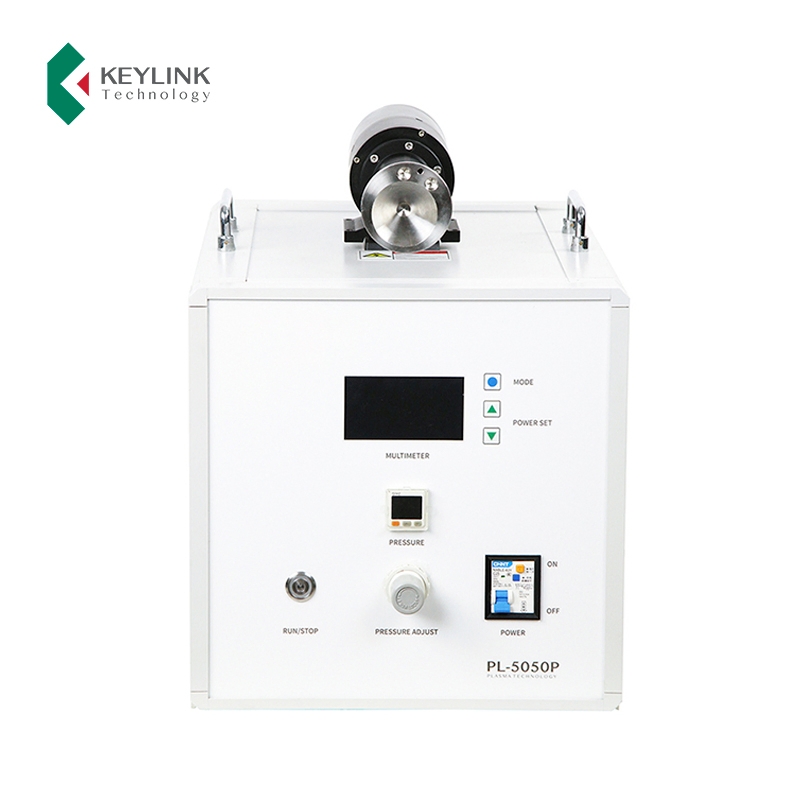
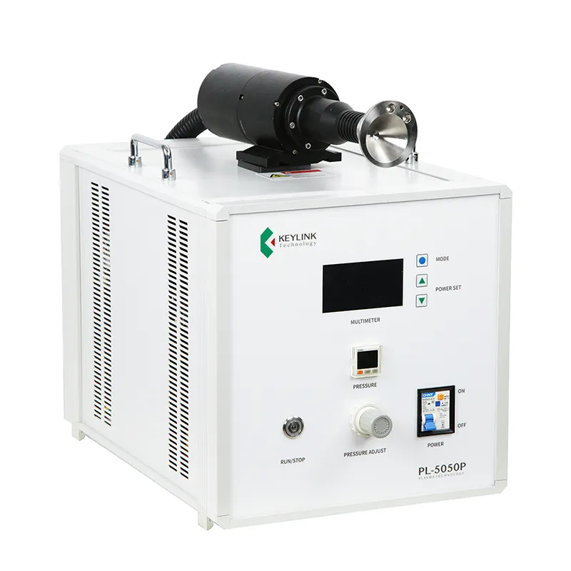
1 / 5

| PL-5050P LCD screen model | |||||
|---|---|---|---|---|---|
| Technical Specification | Nozzle Models | Treatment Area | Model | ||
| Interface Display | 4.3-inch LCD screen | R17 Rotate nozzle | 16mm | PL-JX-022-1 | |
| Rated Voltage | AC220V ±10% | R03 Rotary nozzle | 20mm | PL-JX-004-1 | |
| Output Power | 750-1500W | R04 Rotary nozzle | 30mm | PL-JX-006-1 | |
| Input Current | 4.0-8.0A | R21 Rotary nozzle | 40mm | PL-JX-008-1 | |
| Frequency | 17.3-30kHz | R05 Rotary nozzle | 50mm | PL-JX-010-1 | |
| Air Source | External (60L/min) | R23 Rotate nozzle | 75mm | PL-JX-014-1 | |
| Input Pressure | ≥0.6Mpa | R19 Rotary nozzle | 85mm | PL-JX-016-1 | |
| Storage Temp | -25ºC to +55ºC | R20 Rotary nozzle | 110mm | PL-JX-018-1 | |
| Cleaning Height | 5-15mm |
|
|||
| Net Weight | 28kg | ||||
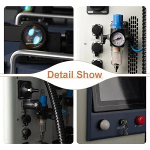
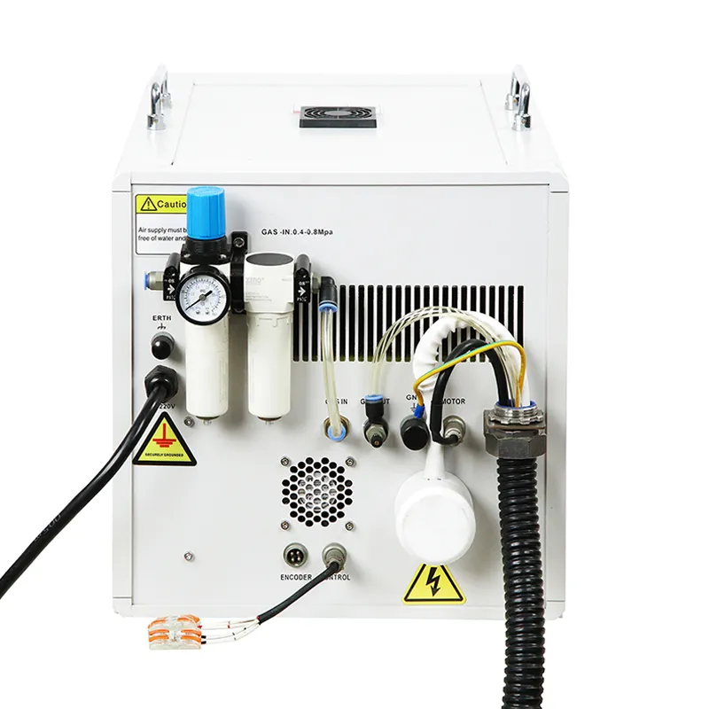
| Detection | Air pressure, temperature, motor speed, driver fault | ||||
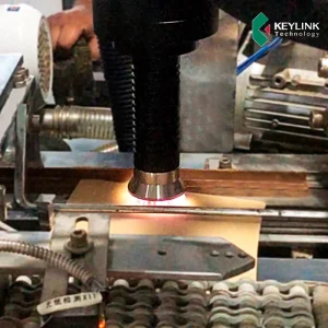
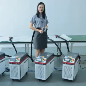
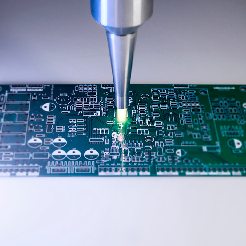
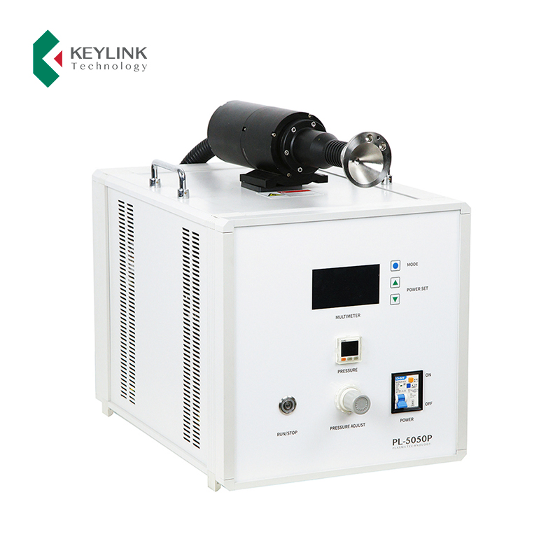
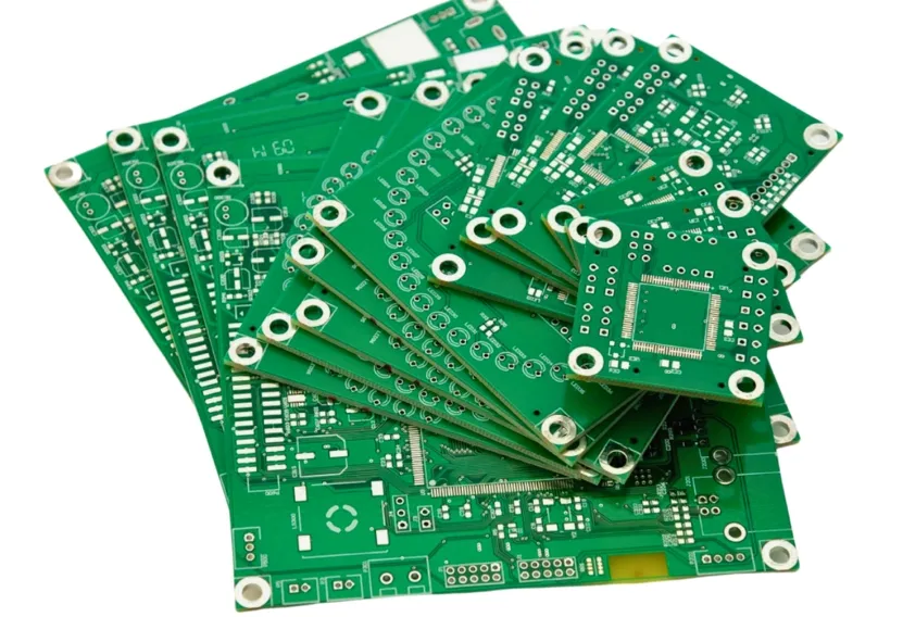
Cleaning a PCB with plasma surface technology offers superior advantages over traditional chemical or ultrasonic cleaning. It provides a microscopic level of decontamination essential for high-reliability electronics.
Atmospheric Plasma: Operates at ambient pressure. Best for removing light organic residues and pre-treatment for coatings in fast inline manufacturing.
Low-Temperature Plasma: Operates under vacuum. Combines chemical and physical sputtering for deep cleaning of stubborn residues like baked flux and photoresist.